
FIGR / UI TEMPLATE
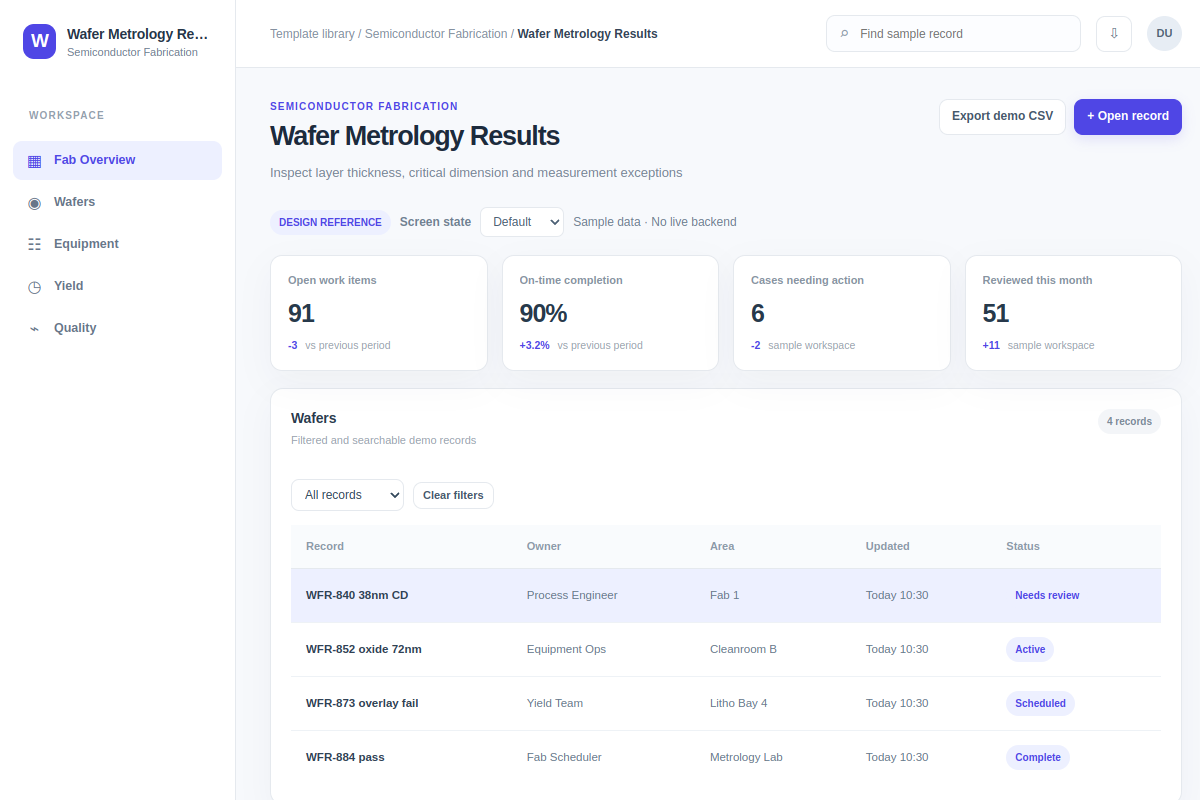
Inspect layer thickness, critical dimension and measurement exceptions.
Explore this table interface for semiconductor fabrication software. Review the workflow and edge cases, then adapt it to your product and design system. All sample records are fictional.
BUILD ON THIS
Explore this screen, then bring in your own product and design system to shape the next version.
Table
Inspect layer thickness, critical dimension and measurement exceptions
table workflow
Default, Selected, Filtered, Empty, Warning, Success
Independent product UI reference
Inspect layer thickness, critical dimension and measurement exceptions.
Core areas: Fab Overview, Wafers, Equipment, Yield and Quality. Show lot records, owners, current statuses and the next step.
Default, Selected, Filtered, Empty, Warning, Success. Include restricted access, missing measurements, blocked work and save failures where relevant.
Fab Overview → Wafer Metrology Results → Inspect layer thickness, critical dimension and measurement exceptions
table, status labels, filters, record details
Keep lot ID, units, thresholds and status visible while users sort and filter. Surface out-of-range measurements.
Preserve tool, lot and approval history. Include timestamps and clear recovery paths if updates fail.
Adapt Wafer Metrology Results to my existing product and design system. Reuse our components, semiconductor workflow, lot traceability and permissions. Explore missing states before creating editable screens.
KEEP EXPLORING
Browse other product UI examples, compare patterns, and pick the direction that suits your product.